The race to dominate the 800V electric vehicle (EV) market is no longer just about battery chemistry; it is a battle of thermal management and power density. As global OEMs and fast-moving Chinese players push the envelope on ultra-fast charging, the demand for highly efficient silicon carbide (SiC) semiconductors has spiked. Addressing this strategic shift, the launch of the new Infineon CoolSiC G2 750V H-DPAK half-bridge devices marks a massive step forward in high-performance automotive power design.
The Battle for Thermal Efficiency in 800V EV Architectures
As a power electronics analyst tracking global EV supply chains, I have seen first-hand how the transition to 800V architectures has exposed the physical limits of traditional packaging. Conventional Bottom-Side Cooling (BSC) forces heat down through the PCB to the heatsink. This significantly limits thermal dissipation, restricts board layout options, and introduces thermal stresses that degrade system reliability over time.
By shifting to Top-Side Cooling (TSC), the H-DPAK package allows the heat to be dissipated directly from the top surface of the chip to an upper heatsink. This thermal decoupling allows design engineers to place components on both sides of the PCB, drastically shrinking the overall system footprint while enhancing reliability. In the hyper-competitive Chinese EV market where 'China-speed' development cycles demand instant hardware optimization, TSC is quickly transitioning from a premium feature to an industry standard.
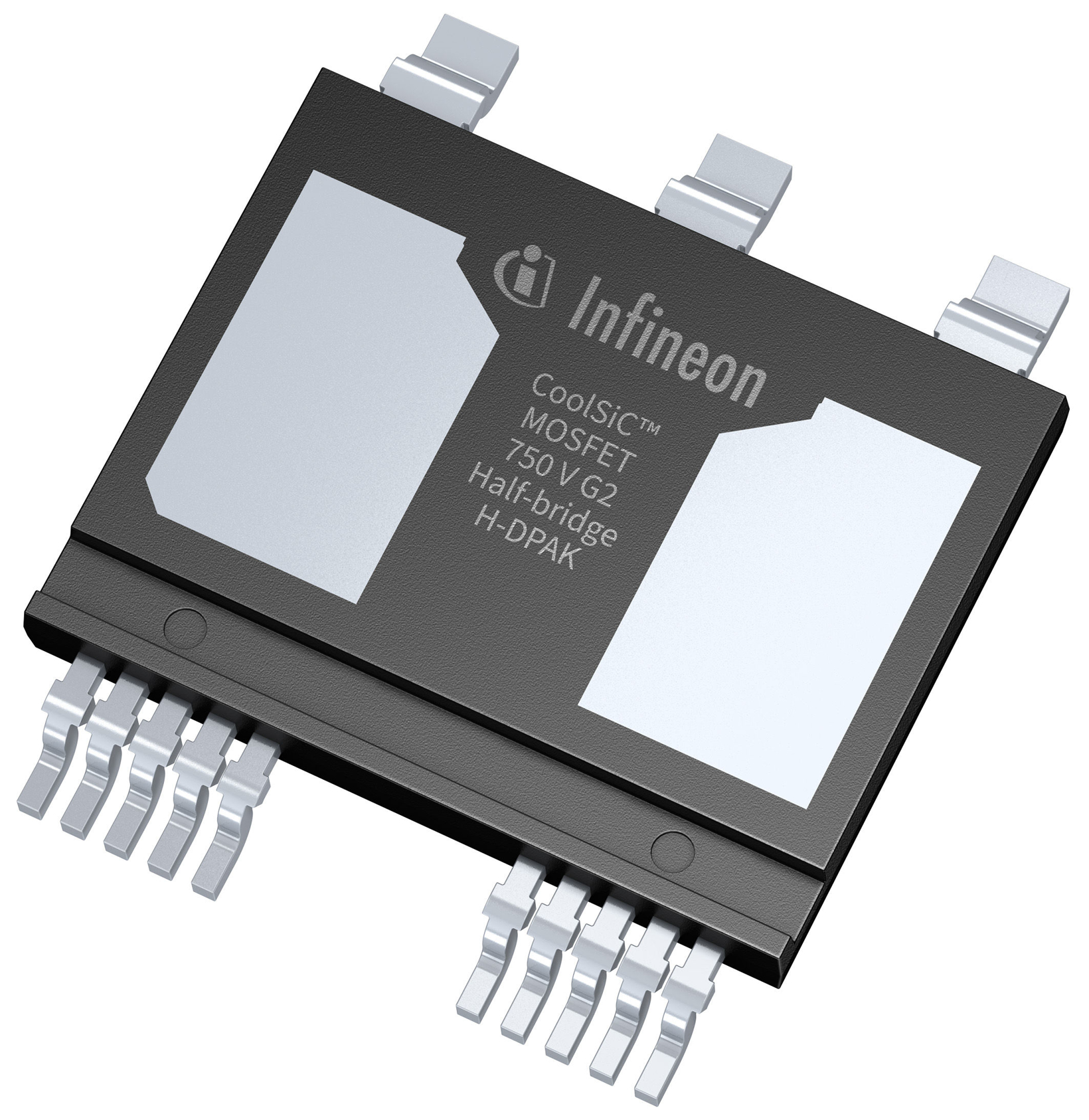
Technical Deep-Dive: Infineon CoolSiC G2 750V H-DPAK
Infineon's integration of its 750V CoolSiC G2 technology into a single half-bridge H-DPAK package solves several structural challenges for Tier 1 suppliers. The split leadframe design combined with an optimized drain pad drastically reduces parasitic inductance while improving creepage and clearance distances required for high-voltage applications.
The table below highlights how Top-Side Cooled H-DPAK modules compare to traditional Bottom-Side Cooled packaging in high-power setups:
| Feature / Parameter | Bottom-Side Cooling (BSC) | Top-Side Cooling (TSC) / H-DPAK |
|---|---|---|
| Thermal Dissipation Path | Through PCB to heatsink (indirect) | Directly to top-mounted heatsink (direct) |
| PCB Utilization | Single-sided component placement | Double-sided component placement enabled |
| Inductive Loop | Higher parasitic inductance | Minimized loop inductance via integrated half-bridge |
| Voltage Rating | 650V standard limit | 750V CoolSiC G2 robust margin |
Strategic Impact on Chinese OEMs and Western Competitors
In China, where companies like BYD, Geely, and Xiaomi are rapidly upgrading their line-ups to 800V platforms (featuring extreme fast-charging metrics), component localization and supply-chain resilience are paramount. Infineon's choice to expand its 750V range is a direct play to secure high-volume design wins against emerging domestic Chinese SiC manufacturers such as Sanan IC and BYD Semiconductor.
For Western OEMs (Tesla, VW, Ford), adopting the Infineon CoolSiC G2 750V platform offers a way to counter China's cost-efficiency advantage. By simplifying thermal system designs, Western manufacturers can lower overall system costs, minimize failure rates, and scale their premium 800V architectures down to mainstream models.