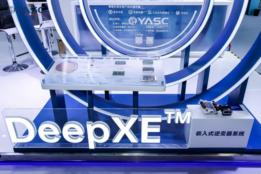
When the global automotive semiconductor crunch crippled vehicle production lines between 2021 and 2023, Beijing treated power electronics not merely as a commercial bottleneck, but as an existential supply chain hazard. Today, China has decisively cleared its first major hurdle: local domestic foundries and crystal growers can reliably synthesize silicon carbide (SiC) boules and fabricate bare SiC MOSFETs at scale. Yet, as domestic semiconductor executives admitted at industry forums this autumn, mastering raw substrate crystallization and wafer slicing was merely the preliminary qualifying round. The real industrial battleground has shifted from basic device fabrication to deep system-level integration—engineering the gate drivers, planar versus trench cell architectures, packaging materials, and real-time firmware necessary to survive high-voltage traction inverter cycles over a fifteen-year automotive lifespan.
For Western automotive executives and semiconductor portfolio managers, the narrative surrounding China silicon carbide EV semiconductors has long swung between two dismissive extremes: either underestimating Chinese device yields as uncompetitive laboratory exercises, or catastrophizing an overnight collapse of Western market share. Both views miss the intricate engineering reality now unfolding across the automotive hubs of Shenzhen, Suzhou, and Munich. Chinese wide-bandgap chipmakers—backed by aggressive Tier-1 EV original equipment manufacturers (OEMs) such as BYD, Geely, and XPeng—are systematically dismantling the historical moats held by European and American power device giants. However, shifting from low-voltage auxiliary converters to main traction inverters under demanding 800-volt charging conditions exposes raw physics limitations that no volume-subsidized price war can immediately solve.
The Engineering Divide: Planar Topologies, Trench Cells, and the 800V Transition
Silicon carbide boasts fundamental physical advantages over traditional silicon-based insulated gate bipolar transistors (IGBTs). Operating with a bandgap three times wider (approximately 3.26 eV for 4H-SiC compared to 1.12 eV for silicon) and a breakdown electric field ten times greater, SiC enables power switches to operate at vastly higher junction temperatures (exceeding 175°C), cut switching losses by upwards of 70 percent, and double inverter switching frequencies. In practical terms for an 800V battery electric vehicle, transitioning from legacy 750V Silicon IGBT modules to 1200V SiC MOSFETs can recover between 4% and 8% of total vehicle battery capacity strictly through efficiency preservation at the traction inverter stage. This enables smaller battery pack sizing without penalizing real-world highway driving range.
Yet moving this electrochemistry into reliable mass-market traction inverters reveals distinct architectural tiers where Western incumbents and Chinese challengers diverge. The overwhelming majority of production-ready China silicon carbide EV semiconductors currently utilize planar MOSFET architectures. Planar gate designs feature an easier manufacturing curve, lower gate-oxide field stress, and more forgiving photolithography tolerances on 6-inch (150mm) substrate lines. However, planar devices suffer from an intrinsically higher specific on-resistance per unit area (Rds(on) x Area). To achieve the low overall resistance demanded by high-output main drive inverters (frequently under 2.0 mΩ per module), Chinese chipmakers must expand the active physical die size. Enlarging the SiC die area exponentially multiplies yield vulnerability due to the inherent micropipe and basal plane dislocation (BPD) defect densities that continue to haunt domestic ingot growth.
Conversely, established Western powerhouses—namely Infineon with its proprietary asymmetric CoolSiC trench cell topology and ROHM with double-trench technology—etch gate channels vertically into the crystal substrate. Trench architectures eliminate the parasitic JFET (junction field-effect transistor) region, reducing the specific on-resistance by 30% to 50% compared to planar equivalents and allowing substantially smaller die dimensions for identical current handling. While domestic Chinese fabricators like Sanan Semiconductor, CRRC Times Electric, and BYD Semiconductor have demonstrated working engineering samples of trench-gate SiC devices in controlled bench evaluations, moving these complex vertical cell structures from pilot runs to high-volume automotive production lines remains a technical bottleneck plagued by gate-oxide reliability under continuous thermal shock and repetitive short-circuit events.
| Parameter / Architecture | Western Tier-1 Benchmark (STMicro / Infineon / onsemi) | Domestic Chinese Production (BYD Semi / Sanan / CRRC) | Automotive Engineering Implication |
|---|---|---|---|
| Primary Cell Topology | Trench Gate (Infineon asymmetric; ST Gen-3/4 advanced planar/trench hybrid) | 1st/2nd Gen Planar MOSFET (Trench currently in pilot/low-volume trial) | Planar requires 20–35% larger die area for equivalent Rds(on), lowering wafer gross margins. |
| Wafer Diameter Base | Transitioning to 8-inch (200mm); Catania & Mohammedia fabs scaling | Dominant 6-inch (150mm); 8-inch pilot lines expanding via SICC & TankeBlue | 8-inch yields lower unit die costs by 20–30% once substrate defect rates fall below 0.5 defects/cm². |
| Specific On-Resistance (Rds(on)*A) | ~1.8 to 2.3 mΩ·cm² (1200V rated) | ~2.8 to 3.5 mΩ·cm² (1200V rated planar) | Higher resistance generates thermal dissipation challenges during peak regenerative braking. |
| Packaging Interconnect | Direct-bonded copper (DBC), planar wire bondless, double-sided direct cooling | Silver sintering adopted; copper wire bonding mainstream; 3D direct-cooling ramping | Silver sintering dramatically extends module lifetime under high power cycling profiles. |
| AEC-Q101 Field History | Over 10+ years of commercial fleet operation and field telemetry | 3 to 5 years limited operational deployment, heavily weighted toward domestic fleet usage | Western OEMs hesitate to qualify Tier-2 Chinese devices due to long-term lifecycle uncertainty. |
The Substrate Crucible and Bill of Materials Reality
To understand the competitive dynamics of China silicon carbide EV semiconductors, one must dismantle the bill of materials (BOM) of a modern 1200V SiC power module. Unlike standard silicon integrated circuits, where the raw substrate accounts for a modest 5% to 8% of the final fabricated wafer cost, the raw monocrystalline SiC substrate accounts for between 35% and 50% of the completed device cost. This discrepancy is governed by the brutal crystal growth kinetics of silicon carbide: physical vapor transport (PVT) growth methods operate inside sealed graphite furnaces at temperatures exceeding 2,400°C, yielding boule growth rates of merely a few millimeters per hour, compared to several meters per day for silicon via the Czochralski process.
Historically, American material pioneers like Wolfspeed (formerly Cree) and Coherent held an effective oligopoly over high-purity single-crystal 4H-SiC boules. However, extensive state-directed capital subsidies and industrial clustering in China have propelled domestic substrate specialists like SICC Co., TankeBlue, and Sanan Optoelectronics to parity in 6-inch substrate mass production. Industry data indicates Chinese domestic 6-inch conductive substrates have experienced severe pricing compression over the past 24 months, with spot market prices tumbling from approximately $800–$900 per substrate down toward $400–$500. This 40% to 50% price decline has eroded the upstream margins of global substrate suppliers, forcing market incumbents to rapidly accelerate their transitions toward 8-inch (200mm) production to preserve operating margins.
However, cost reduction at the substrate level does not instantly translate into parity at the complete traction inverter tier. A complete power stage involves sophisticated silver sintering die-attach techniques, silicon nitride (Si3N4) active metal brazing (AMB) ceramic substrates, low-inductance terminal leads, and specialized high-speed gate driver ICs capable of delivering peak switching speeds without triggering excessive electromagnetic interference (EMI) or severe dV/dt transient voltage spikes. While Chinese packaging facilities have successfully adopted pressure-assisted silver sintering—raising thermal conductivity from approximately 60 W/mK for traditional tin-lead solders to over 200 W/mK—many advanced peripheral components, including galvanic isolators and precision high-voltage gate drivers, remain heavily dependent on Western suppliers such as Texas Instruments, Analog Devices, and Broadcom.
Disruption, Substitution, and Margin Warfare in Global Supply Chains
The acceleration of China silicon carbide EV semiconductors creates diverging trajectories across the global automotive supply chain. The clear beneficiaries are domestic Chinese electric vehicle manufacturers executing extreme vertical integration strategies. BYD, via its internal BYD Semiconductor division, operates proprietary end-to-end substrate, fabrication, module packaging, and vehicle integration lines. This captive integration allows BYD to optimize power electronics directly for its Blade battery pack and e-Platform 3.0 architectures, stripping out commercial markups and driving down the marginal cost of 800V vehicle architectures into price brackets under 200,000 RMB ($28,000 USD)—a price point where Western OEMs struggle to turn a profit even on 400V silicon-based platforms.
Conversely, Tier-1 semiconductor suppliers face structural margin erosion in mainland China. STMicroelectronics, which secured early architecture design wins across Tesla's Model 3 and Model Y traction inverters, has seen domestic competitors aggressively pitch localized replacement modules to Chinese passenger vehicle programs. In response, STMicroelectronics established an expansive $3.2 billion 200mm SiC manufacturing joint venture in Chongqing with Sanan Optoelectronics—a calculated strategic move designed to protect domestic Chinese OEM relationships by utilizing Sanan's local substrate supply while retaining STMicro's core proprietary device intellectual property. Similarly, onsemi, Infineon, and Bosch are engaged in parallel dual-sourcing strategies, retaining high-spec European and American vehicle platform allocations while partnering or localizing within China to defend their market share against domestic substitution mandates.
The structural losers in this evolving landscape are merchant silicon carbide suppliers lacking either captive automotive volume or sovereign capital subsidies. Non-vertically integrated wafer foundries unable to maintain high yields face an intense margin squeeze. As Chinese domestic OEMs increasingly mandate Tier-2 semiconductor dual-sourcing—specifying at least one qualified domestic SiC device alongside an international incumbent—un-differentiated European and American power device suppliers without proprietary trench topologies or deep Tier-1 packaging partnerships face displacement from China's rapidly growing EV volume segments.
The Reality Check: Physics, Packaging, and the Yield Illusion
Despite aggressive domestic marketing and triumphant announcements regarding Chinese SiC self-sufficiency, a rigorous engineering evaluation reveals significant constraints between foundry announcements and mass-production performance. Moving high-voltage semiconductors from laboratory test benches to passenger vehicles introduces harsh thermal, chemical, and mechanical stress cycles that expose fundamental material defects.
The first engineering constraint lies in substrate defect distribution during the transition from 6-inch to 8-inch crystal boules. While domestic Chinese crystal growers have demonstrated 8-inch SiC substrates at industrial exhibitions, independent metallurgical analyses confirm that defect densities—specifically basal plane dislocations (BPDs), threading edge dislocations (TEDs), and micro-cracks—remain elevated on preliminary Chinese 8-inch material compared to mature Western lines. In a power MOSFET, a single active-area BPD can transform under continuous forward voltage bias into a Shockley-type stacking fault, permanently expanding the on-state resistance, causing localized hot spots, and eventually triggering catastrophic thermal runaway. Claims that China has completely achieved commercial 8-inch SiC maturity gloss over the low die-yield realities that make domestic 8-inch production cost-inefficient outside state-supported commercial initiatives.
The second engineering reality involves the gap between manufacturing a standalone SiC switch and successfully deploying a fully integrated system-level traction inverter. As emphasized in the underlying industry telemetry, fabricating a functional chip is only half the equation; system-level implementation requires solving extreme high-voltage transient challenges. SiC MOSFETs switch at speeds exceeding 50 to 100 kilovolts per microsecond (kV/μs). At these switching rates, stray inductances inside the power module packaging as minute as 5 nanohenries (nH) will induce massive voltage spikes (V = L * di/dt) that will breach the gate oxide layer and destroy the device. Western incumbents have spent decades developing proprietary, low-inductance transfer-molded packaging techniques and integrated short-circuit desaturation detection circuits that shut down gate drivers within a fraction of a microsecond. Domestic Chinese inverter assemblers, often rushing to meet shortened OEM design cycles, are struggling with system-level parasitic resonance, severe electromagnetic noise, and unproven long-term gate-oxide degradation profiles over 100,000-mile endurance profiles.
Finally, the automotive qualification barrier remains substantial. Securing AEC-Q101 component qualification and OEM-specific mission profile validations requires running thousands of units through High Temperature Reverse Bias (HTRB), High Temperature Gate Bias (HTGB), and intermittent operating life (IOL) cycling for thousands of hours under extreme ambient temperatures. Passing accelerated lab tests is fundamentally different from surviving decade-long thermal cycling through harsh northern winter sub-zero starts and aggressive summer DC fast charging. Most domestic Chinese SiC power devices have only entered mass-production vehicles within the last three to four years, leaving their long-term field reliability unproven compared to the decades of real-world operational data amassed by legacy competitors.
Inside the Physics: Why SiC Mass Production Faces Steep Hurdles
While domestic foundries claim volumetric maturity on 6-inch wafers, scaling to 8-inch faces a brutal yield cliff driven by basal plane dislocation (BPD) defects. A single micropipe can trigger thermal runaway under continuous forward bias, rendering high-voltage traction inverters unreliable without advanced defect screening that remains unproven at scale.
System integration lags behind raw fabrication; Chinese planar architectures require larger die areas compared to Western trench topologies, increasing cost and heat dissipation challenges. Without verified AEC-Q101 field data spanning 15-year lifecycles, OEMs hesitate to replace proven silicon incumbents with untested domestic SiC modules despite the theoretical efficiency gains.
Strategic Outlook and Investor Implications
The progression of China silicon carbide EV semiconductors from basic device manufacturing to advanced system integration will dictate the distribution of enterprise value and operational profitability across both Western and Asian power semiconductor sectors over the remainder of this decade.
Bull Case
In this scenario, Chinese substrate and device manufacturers successfully reduce 8-inch SiC defect densities below 0.3 defects/cm² while transitioning their proprietary planar architectures to reliable, commercial-grade vertical trench topologies within 24 to 36 months. Captive domestic OEM scale enables Chinese chipmakers to optimize their system-level packaging, integrate localized gate drivers, and capture more than 60% of the domestic Chinese automotive traction inverter market. STMicroelectronics, onsemi, and Infineon are relegated strictly to premium export models and Western domestic platforms, while Chinese Tier-1 suppliers begin securing major power electronics platform wins across emerging automotive manufacturing hubs in Southeast Asia, Latin America, and Europe through compliant localized assembly.
Base Case
China maintains overwhelming cost dominance across 6-inch conductive SiC substrates and captures a significant share of the domestic mass-market (sub-$30,000) 800V EV segment utilizing mature planar MOSFET designs and third-party packaging. However, Western incumbents retain their technology moats in high-reliability trench architectures, advanced integrated power modules, and specialized gate driver ecosystems. Global OEMs continue to mandate Western power semiconductors for their international architectures due to AEC-Q101 field pedigree and export compliance, resulting in a fractured global power semiconductor ecosystem characterized by domestic Chinese dual-sourcing on one side, and Western supply chains prioritizing higher-margin industrial, renewable energy, and premium EV programs on the other.
Bear Case
Long-term field reliability failures and latent gate-oxide degradation issues emerge across early-generation Chinese planar SiC inverters, prompting costly automotive recalls and stalling domestic OEM substitution programs. Meanwhile, global overcapacity in low-tier 6-inch SiC substrates triggers an intense price war among domestic Chinese crystal growers, bankrupting several state-subsidized wafer startups. Western semiconductor incumbents accelerate their 8-inch cost-reduction roadmaps, widening the structural efficiency gap via next-generation trench designs and preserving their leadership across both top-tier Chinese export vehicles and global automotive platforms.
For equity analysts, institutional investors, and Tier-1 automotive procurement strategists, the critical indicators over the next 18 months do not hinge on raw wafer production claims. Survival and competitive advantage will be measured by certified wafer defect densities on 8-inch lines, field-validated thermal cycling telemetry in continuous 800V real-world operation, and the engineering maturity of the module gate driver ecosystem required to turn bare SiC switches into reliable automotive propulsion systems.