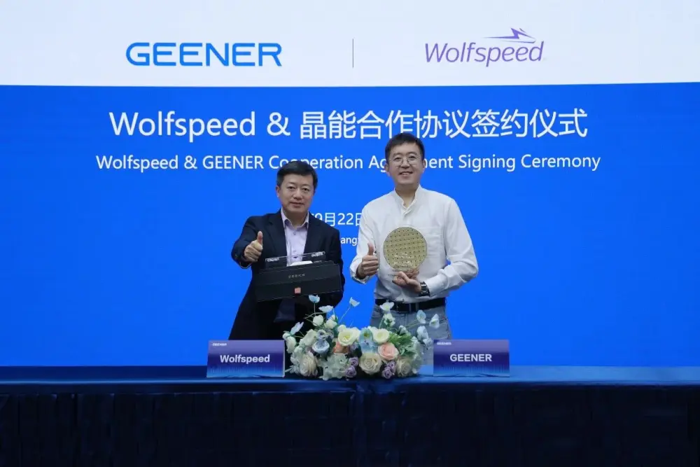
When Wolfspeed (NYSE: WOLF) and Geener Microelectronics (晶能微电子), the dedicated power semiconductor division incubated under Zhejiang Geely Holding Group, executed a Memorandum of Understanding (MOU) in Hangzhou, the headline appeared to signify another standard commercial tie-up in the high-voltage automotive transition. Yet beneath the sanitized corporate announcements lies a pivotal development for Silicon Carbide EV powertrains. At a time when cross-border semiconductor partnerships between American foundries and Chinese automotive conglomerates are facing unprecedented scrutiny, this alliance exposes both the technological dependencies of Chinese OEMs racing to scale 800-volt battery architectures and the desperate search for stable automotive volume by Western wide-bandgap (WBG) chipmakers.
From our analysis of Hangzhou and North Carolina supply chain telemetry, the automotive power semiconductor landscape is entering a fractured phase. Automakers can no longer treat power discretes as fungible commodities. The transition from legacy 400-volt silicon Insulated Gate Bipolar Transistors (IGBTs) to 800-volt planar and trench SiC MOSFETs directly determines vehicle charging curves, inverter efficiency, thermal dissipation volume, and ultimately, battery pack sizing. As Geely accelerates 800V rollouts across its Zeekr, Lotus, Polestar, Smart, and Galaxy platforms, securing reliable automotive-grade SiC bare die is an existential operational imperative.
The High-Voltage Paradigm: Engineering Silicon Carbide EV Powertrains
To grasp why Geener Microelectronics is pursuing Wolfspeed's raw materials, one must examine the engineering physics of inverter topology in modern electric vehicles. In a conventional 400V inverter utilizing silicon IGBTs paired with fast-recovery diodes, conduction and switching losses account for roughly 8% to 10% of total pack energy consumption under typical WLTP/CLTC operating cycles. Moving to high-voltage Silicon Carbide EV powertrains operating between 750V and 900V fundamentally changes inverter thermodynamics.
Silicon Carbide possesses a critical breakdown electric field of approximately 2.8 MV/cm—nearly an order of magnitude higher than silicon's 0.3 MV/cm. This wide bandgap (3.26 eV for 4H-SiC compared to 1.12 eV for silicon) allows for dramatically thinner drift layers and higher dopant concentrations for a given breakdown voltage rating (typically 1200V for 800V architectures). Consequently, the specific on-state resistance (R_DS(on) * Area) drops precipitously. When integrated into Geener’s automotive-grade packaging lines, Wolfspeed’s SiC MOSFET dies deliver switching energy loss reductions exceeding 65% compared to baseline silicon solutions.
Geener Microelectronics is not an integrated device manufacturer (IDM) that produces its own SiC crystal ingots. Instead, Geener focuses on downstream module packaging, direct liquid-cooling baseplates, sintered silver die-attach technology, and copper wire bonding designed to withstand thermal cycles up to 175°C junction temperatures (T_j). Pairing Geener's packaging designs with Wolfspeed's 1200V bare-die MOSFETs aims to yield dual-inverter drive units delivering peak output currents exceeding 600A with inverter power densities exceeding 40 kW/L. However, packaging high-power SiC dies introduces extreme dv/dt switching transients (frequently exceeding 50 V/ns), demanding ultra-low parasitic inductance in the power loop (sub-5 nH) to avoid catastrophic voltage overshoots that puncture gate oxides.
| Metric / Specification | Wolfspeed / Geener Architecture | STMicroelectronics (Tesla Baseline) | onsemi (Hyundai E-GMP Platform) | BYD Semiconductor (In-House SiC) |
|---|---|---|---|---|
| Wafer Diameter Standard | 200mm (8-inch) Transitioning | 150mm (6-inch) / 200mm Planned | 150mm (6-inch) / 200mm Transitioning | 150mm (6-inch) Domestic Dominant |
| MOSFET Voltage Rating | 1200V (Targeted for 800V Systems) | 650V - 750V (Dual 400V Config) | 1200V EliteSiC Modules | 1200V Trench / Planar Mix |
| Die Attach Technology | Sintered Silver / Direct Bond Copper | Advanced Diffusion Soldering | Sintered Die Attach | Silver Sintering / DBC Substrate |
| Estimated Inverter Efficiency | 98.5% - 99.1% Peak | 97.5% - 98.2% | 98.4% - 98.8% | 98.0% - 98.5% |
| Primary Architectural Focus | Zeekr 001/007/009, Lotus Eletre, Galaxy | Model 3 / Model Y Drive Units | Ioniq 5 / Ioniq 6 / EV6 / Genesis | Han, Tang, Denza, Yangwang Architectures |
Supply Chain Architecture: Wafer Yields, Substrates, and BOM Realities
The core commercial driver behind this MOU lies in the Bill of Materials (BOM) economics of power electronics. A standard dual-motor EV utilizing silicon IGBTs carries an inverter BOM cost of roughly $350 to $450. Upgrading that same drivetrain to high-voltage Silicon Carbide EV powertrains pushes inverter BOM costs upwards of $800 to $1,100, driven largely by the high cost of SiC substrates and epitaxial wafer processing. Automakers justify this 2x to 2.5x component cost delta through total system optimization: a 6% to 8% efficiency boost permits decreasing battery pack size by 5 kWh to 8 kWh while maintaining equivalent driving range, saving between $500 and $800 in high-nickel LFP or NCM cell procurement costs.
Yet these economics only pencil out if wafer substrate costs decline. Wolfspeed's massive multi-billion-dollar investments in the Mohawk Valley Fab (Marcy, New York) and the John Palmour Manufacturing Center for Silicon Carbide (Siler City, North Carolina) were predicated on a swift migration from 150mm (6-inch) to 200mm (8-inch) wafers. Mathematically, moving from a 150mm to a 200mm wafer increases usable surface area by approximately 77%, cutting the per-die manufacturing cost significantly once fab yields exceed 70%.
Geener Microelectronics is acutely aware of the global substrate supply bottleneck. While Chinese substrate suppliers such as SICC Co., TankeBlue, and Sanan Optoelectronics have poured capital into domestic crystal growth facilities, their high-volume output remains primarily concentrated in 150mm substrates, with 200mm domestic production yields still maturing in baseline defect densities (such as micropipes and threading screw dislocations). By signing an MOU with Wolfspeed, Geely seeks a strategic hedge: securing tier-1 American 200mm bare-die capacity for its export-oriented, premium vehicle brands, while simultaneously utilizing domestic Chinese suppliers for lower-margin domestic nameplates.
Competitive Impact: OEM Margin Pressure and Tier-1 Power Shifts
The alliance between Wolfspeed and Geely’s subsidiary sends ripples across both the semiconductor and automotive landscape, shifting competitive leverage between Western IDMs and vertically integrated Chinese OEMs.
For Western power semiconductor incumbents such as STMicroelectronics, onsemi, and Infineon Technologies, this partnership confirms that Geely is unwilling to surrender its module packaging margin to traditional Tier-1 suppliers like Bosch or BorgWarner. By empowering Geener Microelectronics to handle module design, integration, and thermal management internally, Geely retains software and hardware control over its inverter gate-drive algorithms while squeezing external suppliers to bare-die margins. STMicroelectronics has already adapted to this reality by entering an $3.2 billion joint venture with Sanan Optoelectronics in Chongqing to build a dedicated 200mm SiC device fab. Wolfspeed's move with Geener is a direct counter-maneuver to avoid being locked out of the world’s largest electric vehicle market.
Conversely, for decoupled global automakers such as Hyundai Motor Group, this escalating capacity battle presents a double-edged sword. Hyundai-Kia, which relies heavily on onsemi and Infineon for its high-performance 800V E-GMP vehicles, enjoys stable supply chains insulated from Chinese regulatory entanglements. However, if Geely successfully scales Geener’s packaged modules across millions of mass-market vehicles—including the budget-conscious Galaxy sub-brand—the cost curve for 800V silicon carbide powertrains could collapse faster than Western legacy OEMs anticipate, erasing the efficiency and charging-speed lead currently enjoyed by Western and Korean electric architectures.
The Reality Check: Fab Execution Delays, MOU Optics, and Physics Constraints
While the corporate press release presents a seamless narrative of cross-border technological synergy, a critical examination reveals severe engineering and financial vulnerabilities on both sides of this agreement. Industry observers must separate non-binding declarations of intent from certified automotive-grade production contracts.
First, Wolfspeed’s operational track record over the past 24 months warrants extreme analytical caution. The company has grappled with grueling production ramp delays at its Mohawk Valley facility, high cash burn rates, and recurring wafer yield complications. Fabricating 200mm SiC boules requires growing silicon carbide crystals at temperatures exceeding 2,400°C via physical vapor transport (PVT) under precise vacuum environments. Unlike silicon, SiC is notoriously brittle, prone to basal plane defects, and mechanically difficult to slice without excessive kerf loss. If Wolfspeed cannot stabilize wafer yields at commercial margins, its projected cost advantages over mature 150mm foundries evaporate, leaving supply-constrained partners like Geener in operational jeopardy.
Second, the MOU is not a binding, long-term procurement agreement with hard minimum take-or-pay volume thresholds. In the power semiconductor sector, automotive OEMs routinely sign bilateral MOUs with multiple competing chip suppliers to engineer artificial price leverage. Geely maintains active supplier dialogues and module testing pipelines with STMicro, Infineon, and domestic champion BYD Semiconductor. Labeling this MOU as a definitive victory for Wolfspeed ignores the reality that Geely could abandon or downscale volume allocations if domestic Chinese SiC players achieve cost parity on 150mm wafers or if Geener's internal yield validation fails.
Finally, the physical limitations of Silicon Carbide EV powertrains are frequently glossed over in marketing briefs. While SiC drastically lowers switching losses, high-frequency operation generates severe electromagnetic interference (EMI) and aggressive motor bearing fluting caused by capacitive leakage currents. Resolving these secondary side effects requires expensive common-mode chokes, insulated ceramic bearings, and sophisticated gate-driver shielding. The total system cost reduction promised by SiC is not guaranteed; it demands immaculate vehicle-level engineering that many rapid-to-market brands struggle to execute reliably under high-stress duty cycles.
Inside the Physics: Why Lab-Scale Efficiency Collapses at Scale
The claimed 98.5%-99.1% inverter efficiency represents peak laboratory conditions, not mass-production reality. While SiC reduces switching losses by over 65%, conduction losses dominate at high currents (600A), demanding aggressive liquid cooling architectures that increase BOM cost and weight. Achieving the projected 40 kW/L power density requires sub-5 nH parasitic inductance loops and direct-to-chip thermal management, which are currently unproven at automotive scale due to manufacturing yield volatility on Wolfspeed's 200mm wafers.
Material science constraints remain the primary barrier; SiC crystal growth is brittle, prone to micropipes that cause wafer breakage during slicing. For this partnership to represent a genuine paradigm shift rather than a marketing exercise, Wolfspeed must demonstrate sustained >70% yield on 8-inch substrates before Geener commits volume. Meanwhile, STMicroelectronics' joint venture with Sanan Optoelectronics in Chongqing signals that Western OEMs are already hedging against supply chain bottlenecks, making the non-binding MOU a tactical hedge rather than a guaranteed supply lock.
Strategic Outlook and Multi-Year Investor Implications
The memorandum between Wolfspeed and Geener outlines a critical junction for the auto industry's semiconductor supply chain. How this relationship evolves will signal whether commercial interdependence in trailing-edge and power electronics can survive systemic geopolitical decoupling.
Bull Case
Wolfspeed rapidly resolves yield and wafer defect hurdles at its Mohawk Valley facility, driving 200mm substrate costs down by 30% over the next 24 months. Geener successfully qualifies these dies across Geely’s entire 800V EV portfolio, securing high-margin, high-volume automotive off-take. Geely widens its operational cost advantage in power electronics against Western legacy OEMs, deploying highly efficient Silicon Carbide EV powertrains across Zeekr and Galaxy at retail prices below $30,000, while Wolfspeed returns to sustained operational cash flow positivity.
Base Case
Wolfspeed's 200mm capacity ramps gradually, but yields remain volatile, preventing rapid cost reduction. Geener utilizes Wolfspeed dies selectively for export-focused, premium models (such as Lotus and high-end Zeekr trims) to comply with international client perceptions, while quietly dual-sourcing 150mm domestic substrates from Sanan Optoelectronics and SICC for high-volume domestic vehicles. The MOU translates into steady, moderate volume orders, but fails to dramatically alter either company's fundamental operating margins amid relentless Chinese domestic price wars.
Bear Case
Escalating trade frictions or expanded export control definitions lead to regulatory bottlenecks on advanced 200mm SiC substrate shipments. Simultaneously, Chinese domestic wafer fabricators rapidly conquer 200mm defect rates, dumping cheap automotive-grade SiC substrates onto the domestic market. Geely exercises its non-binding status to abandon Wolfspeed in favor of subsidized domestic suppliers, leaving Wolfspeed saddled with unutilized fab capacity and Geener grappling with localized packaging redesigns.
Strategic Takeaways for Automotive Executives & Investors:
- Vertical Integration of Packaging is Non-Negotiable: Geely's deployment of Geener proves that major OEMs view module packaging, thermal sintering, and gate-driver optimization as proprietary competitive moats, leaving merchant chip suppliers relegated to bare-die component pricing.
- The 200mm Migration Defines SiC Margin Viability: Without achieving sustained commercial yields on 200mm wafers, Western SiC manufacturers cannot maintain pricing power against rapidly expanding 150mm state-backed Chinese substrate foundries.
- MOU Announcements Mask Hedging Strategies: Analysts must heavily discount non-binding corporate MOUs in the EV semiconductor sector; they frequently represent multi-sourcing tactical hedges rather than locked capital expenditure commitments.
- System BOM vs. Inverter Cost Realism: Silicon carbide adoption is not an automatic margin positive; its economic justification relies entirely on an automaker's ability to extract battery pack size savings through superior vehicular thermal and powertrain efficiency.