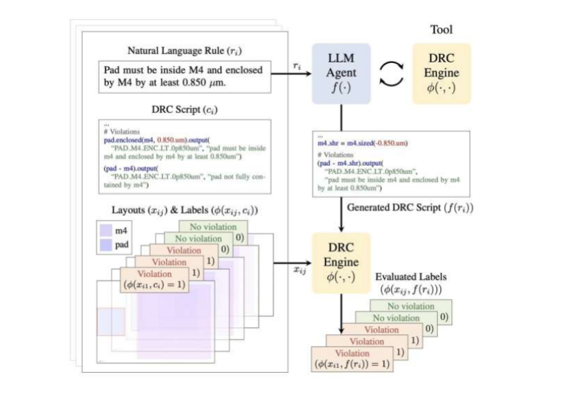
The global race for smarter, more efficient automotive chips is entering a highly automated phase. As automotive architectures shift toward centralized computing and advanced driver-assistance systems (ADAS), the demand for complex, custom silicon has skyrocketed. Addressing this bottleneck, researchers from Seoul National University (SNU) and the Samsung AI Center have pioneered a breakthrough in semiconductor design verification automation by leveraging AI agents to auto-generate Design Rule Checking (DRC) scripts.
The DRC Bottleneck in Next-Gen Automotive Silicon
Before any integrated circuit (IC) goes to a foundry for manufacturing, it must undergo Design Rule Checking (DRC). This step ensures the chip design strictly complies with the physical manufacturing limits of the foundry (such as TSMC, Samsung, or SMIC). Historically, translating thousands of pages of PDF-based foundry design rules into executable DRC scripts has been a tedious, manual coding task performed by highly specialized layout engineers.
As an industry analyst observing the automotive sector, this manual bottleneck has long delayed the time-to-market for custom ASICs and power semiconductors. A single error in a manual script can lead to a multi-million dollar spin-out failure or delayed automotive launches.
Samsung and SNU's Breakthrough: AI Agent-Led Scripting
The joint research team led by Professor Hyun Oh Song at SNU, in collaboration with Samsung AI Center, has introduced a highly specialized AI framework. This AI agent acts as a virtual EDA (Electronic Design Automation) engineer. It reads natural language foundry manuals, understands complex spatial geometry, and automatically outputs syntactically correct DRC scripts.
Crucially, this technology moves beyond basic large language models (LLMs) which often struggle with spatial layout logic and precise code structures. By training the AI agents on specialized semiconductor domain knowledge, the system achieves unprecedented accuracy in automated code generation.
Accelerating EV and Autonomous Driving Chip R&D Cycles
The implications for the electric vehicle (EV) and ADAS sectors are profound. Automotive chips must meet rigorous safety and reliability standards (such as ISO 26262). By adopting semiconductor design verification automation, automotive chip designers can:
- Iterate Faster: Rapidly prototype custom neural processing units (NPUs) for local AI perception models.
- Reduce Development Costs: Free up expensive human layout engineers to focus on higher-level system architecture rather than debugging rule check files.
- Optimize Power Electronics: Speed up the verification of next-generation Silicon Carbide (SiC) and Gallium Nitride (GaN) power semiconductors essential for 800V fast-charging architectures.
Comparative Analysis: Manual vs. Automated Semiconductor Verification
The table below highlights the performance shift expected as these AI agents integrate into mainstream EDA workflows:
| Metric | Traditional Manual DRC Scripting | AI-Agent Verification Automation |
|---|---|---|
| Processing Time | Weeks to Months | Minutes to Hours |
| Error Sensitivity | High (prone to human typo/interpretation errors) | Low (consistent logical translation) |
| Scalability | Poor (requires recruiting more specialized engineers) | Excellent (instantly scalable API calls) |
| Foundry Portability | Requires full script rewrite for new foundries | AI dynamically adapts to new foundry manual PDFs |
Strategic Implications for the Global Automotive Supply Chain
In the highly competitive EV space, rapid silicon development is a core differentiator. The ability to deploy customized, domain-specific hardware ahead of competitors allows EV makers to achieve higher efficiency and better compute performance per watt. Through close technological integration and cross-border collaboration, global technology players are leveraging such automation breakthroughs to build reliable, high-yield chip design frameworks.
For Western automotive brands and tech investors, watching these underlying EDA advancements is critical. It indicates that the barrier to entry for custom silicon design is dropping rapidly, enabling faster localized product iterations globally.