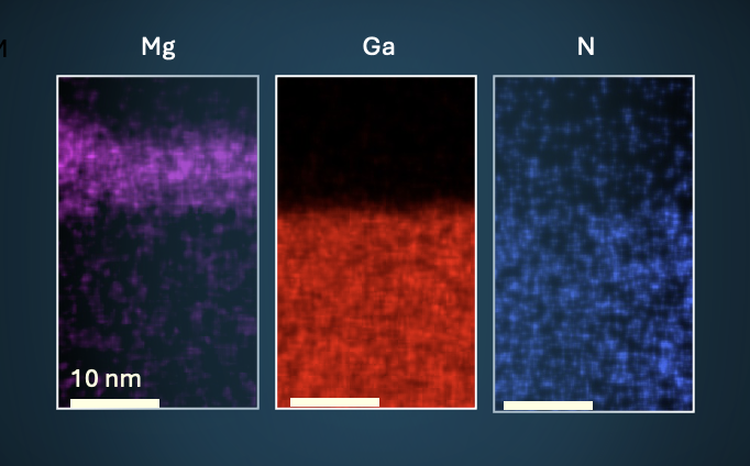
As the automotive industry transitions to 800V architectures and ultra-fast charging, wide-bandgap materials are rapidly replacing legacy silicon. While Silicon Carbide (SiC) has dominated initial high-voltage traction inverter designs, GaN power semiconductors in EVs are emerging as the next frontier for power density and efficiency. However, Gallium Nitride (GaN) has long been held back by a critical material science bottleneck: high contact resistance in p-type semiconductors. A pioneering research team at Nagoya University has recently developed a novel low-resistance contact method, clearing a major path for high-performance GaN power electronics in the global automotive supply chain.
The Nagoya University Breakthrough: Solving the P-Type GaN Bottleneck
Semiconductor devices, including LEDs and transistors, rely on two complementary regions: the n-type region (which carries negative charges via electrons) and the p-type region (which carries positive charges via holes). In GaN-based electronics, creating high-quality, low-resistance electrical contacts on p-type GaN has been an industry-wide challenge for decades.
Due to the inherent material properties of p-type GaN, traditional metal contacts often lead to high contact resistance. This causes significant energy dissipation as heat, limiting the operating frequency and overall efficiency of the semiconductor. The Nagoya University research group addressed this issue by introducing an innovative surface treatment and contact layer deposition process. By dramatically lowering the contact resistance, the team has paved the way for vertical GaN power devices to operate at their theoretical performance limits.
Why This Matters for the EV Power Electronics Ecosystem
As a market analyst closely tracking global powertrain trends, it is clear that efficiency gains in power electronics translate directly into vehicle range and reduced thermal management costs. The application of GaN power semiconductors in EVs holds major advantages over both legacy Silicon (Si) and current-generation Silicon Carbide (SiC):
- Higher Switching Frequencies: GaN switches up to ten times faster than silicon, allowing passive components like inductors and capacitors to be dramatically downsized.
- Reduced On-Board Charger (OBC) Footprint: Leveraging advanced GaN devices can reduce the volume and weight of OBCs and DC-DC converters by up to 60%.
- Enhanced Thermal Efficiency: Low-resistance contacts mean less heat generation, reducing the dependency on complex, heavy liquid cooling loops inside the power distribution unit.
Material Comparison: Si vs. SiC vs. GaN
To understand where GaN fits into the future EV value chain, we can compare its fundamental physical properties to other common semiconductor substrates:
| Material Property | Silicon (Si) | Silicon Carbide (4H-SiC) | Gallium Nitride (GaN) |
|---|---|---|---|
| Bandgap (eV) | 1.1 | 3.2 | 3.4 |
| Electron Mobility (cm²/Vs) | 1,400 | 900 | 2,000 |
| Critical Electric Field (MV/cm) | 0.3 | 3.0 | 3.3 |
| Primary EV Application | Low-voltage auxiliary | Main Traction Inverter | OBC, DC-DC, Fast Chargers |
Strategic Implications for Global OEMs and Suppliers
From a global supply chain perspective, this research represents more than a localized academic milestone. Japan has long held foundational strength in semiconductor materials research, while manufacturing hubs in China and the West excel in large-scale commercialization and vehicle integration.
By resolving the p-type contact resistance limit, vertical GaN structures (which offer higher power handling capabilities than lateral GaN structures) become commercially viable. Global Tier-1 suppliers like Bosch, Denso, and Marelli are actively looking to diversify their wide-bandgap portfolios to mitigate SiC wafer supply constraints. Advancements in vertical GaN architectures provide these system integrators with a high-efficiency alternative, enabling strategic localization and supply chain resilience amidst fluctuating global raw material markets.
The Road to Commercial Automotive Integration
While the laboratory results from Nagoya University are highly promising, translating this material science breakthrough into automotive-grade components typically takes three to five years. The technology must first undergo rigorous AEC-Q101 qualification standards to prove long-term reliability under high-vibration and extreme temperature conditions typical of EV engine bays.
Nevertheless, for automotive strategists and technology investors, this development signals that GaN is rapidly maturing. No longer confined to consumer electronics fast chargers, GaN power semiconductors in EVs are positioning themselves as a essential pillar of future premium EV architectures, enabling lighter, faster-charging, and more aerodynamically optimized vehicles.